エレクトロニクス関連商品のオンラインストア

6インチSiCウェハ 6INCH SIC WAFER

売り手 TYK
定価 ¥2,000,000
販売価格 ¥2,000,000 定価
販売 ASK
単価
/対して 
スタイル:
6 inch 3C-N・P-type SiC Wafer
Properties Specification
Production Grade
(P Grade)
Research Grade
(R Grade)
Dummy Grade
(D Grade)
Diameter 145.5 mm~150.0 mm
Thickness 350 μm ± 25 μm
Wafer Orientation Offaxis:2.0°-4.0°toward[1120]±0.5°for 4H/6H-P,
On axis:[111]±0.5°for3C-N
Micropipe Density* 0 cm-2
Resistivity* p-type 4H/6H-P ≤0.1 Ω·cm ≤0.3 Ω·cm
n-type 3C-N ≤0.8 mΩ·cm ≤1 m Ω·cm
Primary Flat Orientation   4H/6H-P {1010} ± 5.0°
  3C-N {110} ± 5.0°
Primary Flat Length 32.5 mm ± 2.0 mm
Secondary Flat Length 18.0 mm ± 2.0 mm
Secondary Flat Orientation Silicon face up: 90° CW. from Prime flat ± 5.0°
Edge Exclusion 3 mm 6 mm
LTV ≤2.5 μm ≤10 μm
TTV ≤5 μm ≤15 μm
Bow ≤15 μm ≤25 μm
Warp ≤30 μm ≤40 μm
Roughness* Polish Ra≤1 nm
CMP Ra≤0.2 nm Ra≤0.5 nm
Edge Cracks By High Intensity Light None Cumulative length ≤ 10 mm, single
length≤2 mm
Hex Plates By High Intensity Light* Cumulative area ≤0.05% Cumulative area ≤0.1%
Polytype Areas By High Intensity Light* None Cumulative area≤3%
Visual Carbon Inclusions Cumulative area ≤0.05% Cumulative area ≤3%
Silicon Surface Scratches By High Intensity Light # None Cumulative length≤1×wafer diameter
Edge Chips High By Intensity Light None permitted ≥0.2mm width and depth 5 allowed, ≤1 mm each
Silicon Surface Contamination By High Intensity None
Packaging Multi-wafer Cassette or Single Wafer Container
Notes:
※ Defects limits apply to entire wafer surface except for the edge exclusion area.
# The scratches should be checked on Si face only.


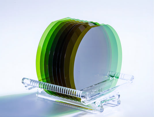
※写真は代表的なSiCウェハ(当該品とは別口径)になります。

※在庫品ではありません。納期・数量は都度お問い合わせください。

予約注文テキスト